Слайд 2
What is S3/S4? And what’s the benefit?
S3/S4 power
system and control sequence?
How to implement S3/S4??
How to debug
S3??
Agenda
Слайд 3
What is S3/S4 ??
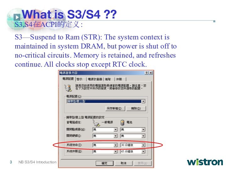
S3,S4在ACPI的定义:
S3—Suspend to Ram (STR): The
system context is maintained in system DRAM, but power
is shut off to no-critical circuits. Memory is retained, and refreshes continue. All clocks stop except RTC clock.
Слайд 4
What is S3/S4 ??
ACPI:
1996 年时,由微软(Microsoft)、英特尔(Intel)与东芝(Toshiba)主导,共同制定了业界以「操作系统」为标准的电源管理程序ACPI(Advanced
Configuration & Power Interface),正式把电源管理工作交给操作系统来负责.
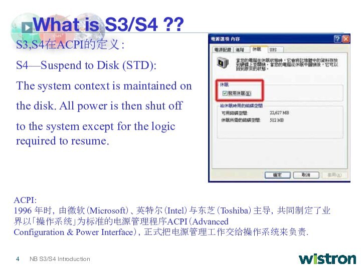
S3,S4在ACPI的定义:
S4—Suspend
to Disk (STD):
The system context is maintained on
the
disk. All power is then shut off
to the system except for the logic required to resume.
Слайд 5
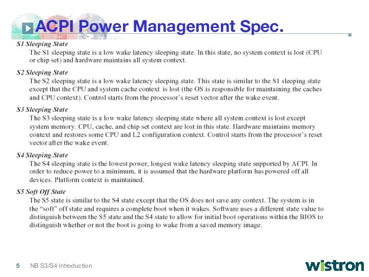
ACPI Power Management Spec.
Sleeping State Definitions:
Sleeping states are
types of sleeping state within global sleeping state, G1
Слайд 6
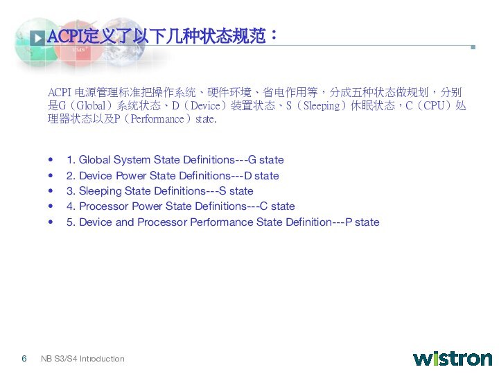
1. Global System State Definitions---G state
2. Device Power
State Definitions---D state
3. Sleeping State Definitions---S state
4. Processor Power
State Definitions---C state
5. Device and Processor Performance State Definition---P state
ACPI定义了以下几种状态规范:
ACPI 电源管理标准把操作系统、硬件环境、省电作用等,分成五种状态做规划,分别是G(Global)系统状态、D(Device)装置状态、S(Sleeping)休眠状态,C(CPU)处理器状态以及P(Performance)state.
Слайд 7
What’s the benefit of S3/S4??
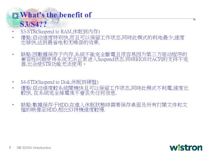
S3-STR(Suspend to RAM,休眠到内存)
優點:启动速度特别快,而且可以保留工作状态,同時此模式的耗电最少,速度也够快,达到最省电和无噪音的效果.
缺點:因數據保存于內存,系統不能完全斷電且很容易因为第三方驱动程序的兼容性问题使得系统无法正常进入Suspend状态.同時BIOS对ACPI的支持不完善,也会使STR功能无法使用。
S4-STD(Suspend to
Disk,休眠到硬盤)
優點:启动速度較系統開機快且可以保留工作状态,同時此模式不耗電,速度也較快, 在系統完全掉電後不會丟失任何信息.
缺點:數據保存于HDD,在進入休眠狀態時需要保存桌面及所有打開文件和文檔的映像至HDD,相比S3待機速度較慢.
Слайд 8
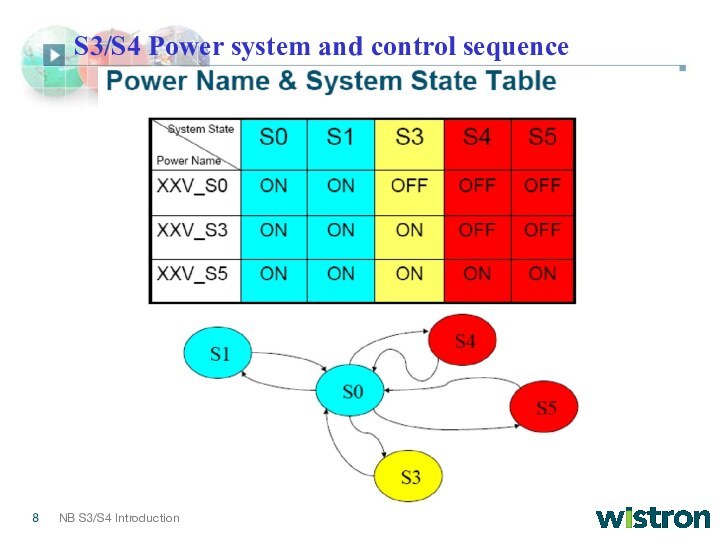
S3/S4 Power system and control sequence
Слайд 12
Power system architecture
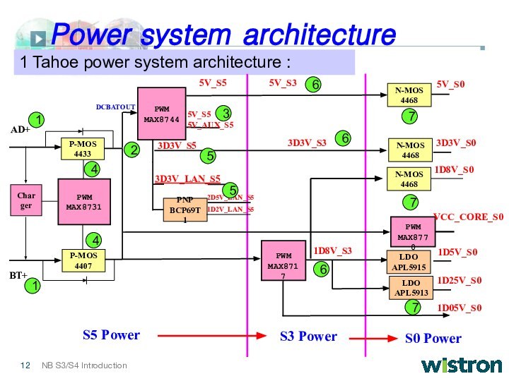
1 Tahoe power system architecture :
PWM
MAX8731
Charger
P-MOS
4407
P-MOS
4433
PWM
MAX8744
PWM
MAX8717
AD+
BT+
N-MOS
4468
N-MOS
4468
5V_S5
5V_AUX_S5
3D3V_S5
DCBATOUT
PNP
BCP69T1
5V_S5
3D3V_S3
5V_S0
3D3V_S0
3D3V_LAN_S5
2D5V_LAN_S5
1D8V_S3
1D5V_S0
LDO
APL5913
1D25V_S0
S5
Power
S3 Power
S0 Power
PWM
MAX8770
VCC_CORE_S0
1D05V_S0
1
4
3
2
1
6
6
5
7
6
4
7
7
5
1D2V_LAN_S5
5V_S3
N-MOS
4468
1D8V_S0
LDO
APL5915
Слайд 13
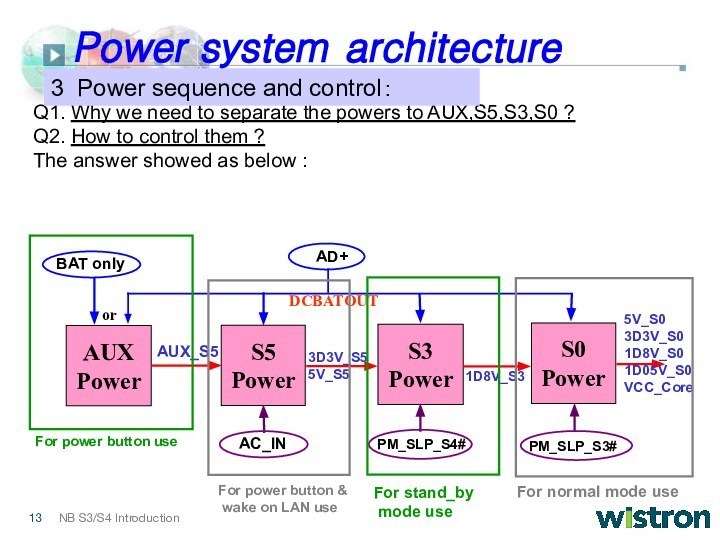
Q1. Why we need to separate the powers
to AUX,S5,S3,S0 ?
Q2. How to control them ?
The answer
showed as below :
AUX
Power
S5
Power
S3
Power
S0
Power
BAT only
AD+
or
AUX_S5
3D3V_S5
5V_S5
DCBATOUT
AC_IN
PM_SLP_S4#
PM_SLP_S3#
1D8V_S3
5V_S0
3D3V_S0
1D8V_S0
1D05V_S0
VCC_Core
For power button use
For stand_by
mode use
For normal mode use
For power button &
wake on LAN use
3 Power sequence and control:
Power system architecture
Слайд 14
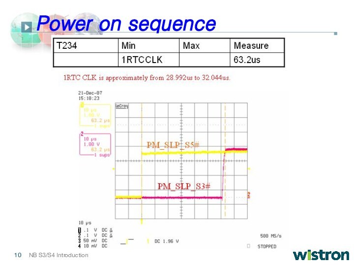
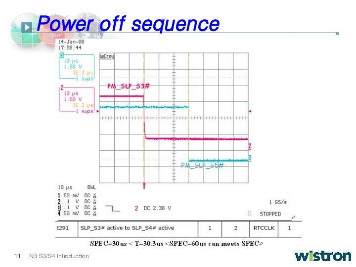
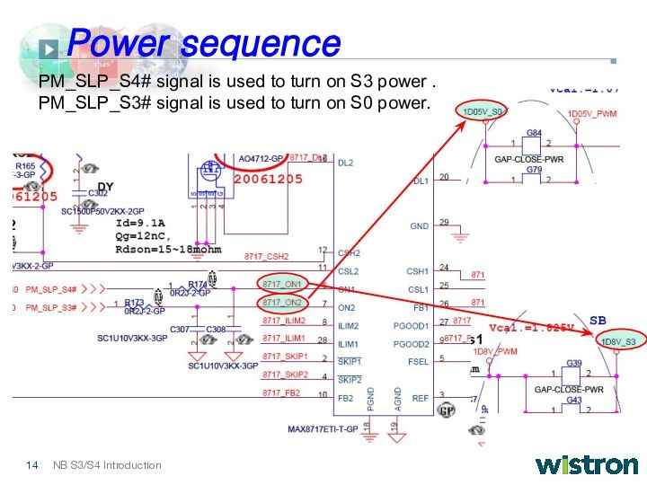
PM_SLP_S4# signal is used to turn on S3
power .
PM_SLP_S3# signal is used to turn on S0
power.
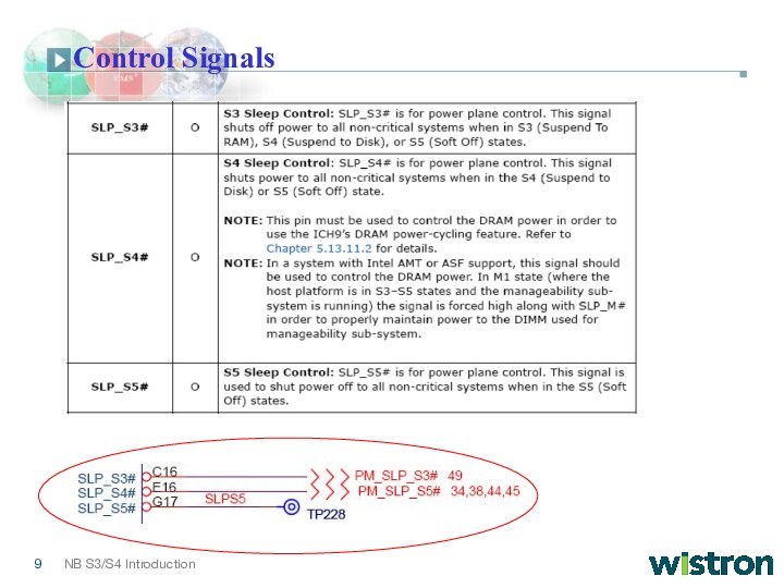
Power sequence
Слайд 15
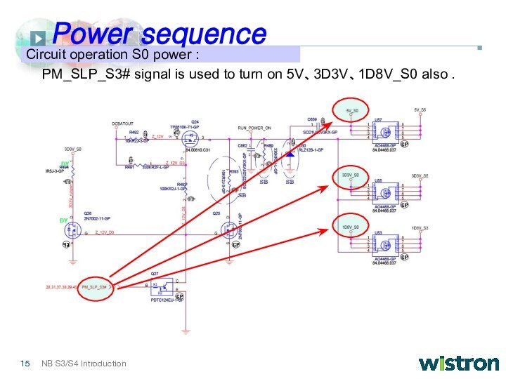
PM_SLP_S3# signal is used to turn on 5V、3D3V、1D8V_S0
also .
Circuit operation S0 power :
Power sequence
Слайд 16
Stand-by动作原理
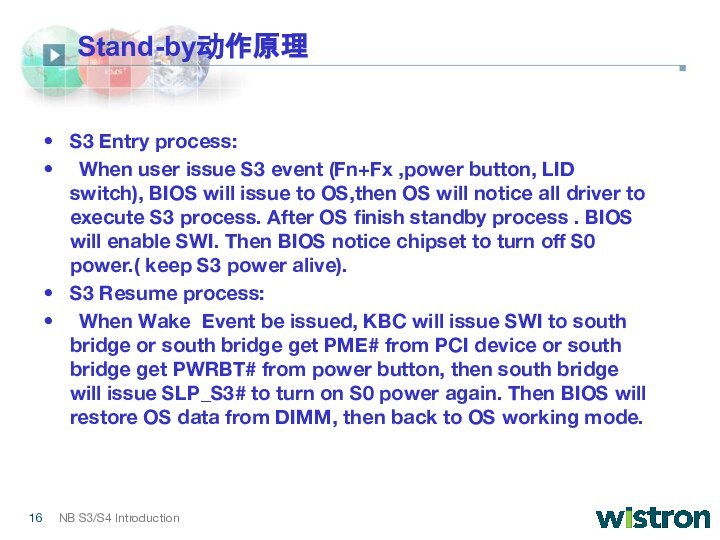
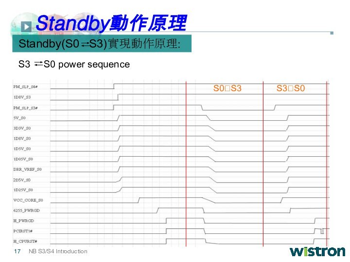
S3 Entry process:
When user issue S3 event (Fn+Fx
,power button, LID switch), BIOS will issue to OS,then
OS will notice all driver to execute S3 process. After OS finish standby process . BIOS will enable SWI. Then BIOS notice chipset to turn off S0 power.( keep S3 power alive).
S3 Resume process:
When Wake Event be issued, KBC will issue SWI to south bridge or south bridge get PME# from PCI device or south bridge get PWRBT# from power button, then south bridge will issue SLP_S3# to turn on S0 power again. Then BIOS will restore OS data from DIMM, then back to OS working mode.
Слайд 17
Standby(S0 S3)實現動作原理:
Standby動作原理
S0?S3
S3?S0
S3
S0 power sequence
Слайд 18
1. 當系統接到Hibernation指令後會將當前文檔,桌面,工作狀態等數據映像寫入HDD內並更改HDD引導區.
2. 所有數據都寫入HDD後系統會依照power off sequence將各reset power依此關掉進入完全關機狀態.
3. S4喚醒時完全follow power
on sequence各power reset會依次打開,CPU正常運作後開始讀取HDD內邏輯引導區引導讀取映像文件,系統恢復到之前狀態.
Standby(S0 S4)實現動作原理:
Hibernation動作原理
Слайд 19
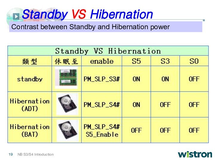
Standby VS Hibernation
Contrast between Standby and Hibernation power
Слайд 20
How to implement S3??
Check SW whether support ACPI
spec.
Check MRS( Marketing Requirement Spec.) support what kind of
S3 wake event.
-Power button,LID,BL2
-USB, WOR,WOL, Any-key wake
-LAN, Card-Bus,IEEE 1394 (PCI PME#)
Check VGA support D3hot or D3cold
Check South Bridge Wake Up Interface
Check KBC Wake Up interface
Check Logic Gate design
Слайд 21
How to implement S3??
Wake Event Design:
USB: If your
system support USB S3 wake,you must provide 5V_S3
for USB power. And BIOS need to enable USB interface S3
wake event.
WOR: If your system support Wake on Ring. You must support S3
power for pin17 of MDC connector. And Vendor’s driver need to
support wake up function.
PCI Device Wake( LAN, Card-Bus, 1394): If your system support PCI
device wake event, you must provide S3 power to AUX power pin
of device. And connect PME# to south bridge’s PME#.
Слайд 22
How to implement S3??
Discrete VGA support D3hot or
D3cold:
D3cold:When system enter S3 state, all power of VGA
will be turn off. But you need to check VGA driver can be supported or not.
D3hot: When system enter S3 state, some graphic power is still alive. It means that S3 power leakage will be increased.
South Bridge Wake Up Interface:
1. Power Button( AUX power plane)
2. SWI from KBC( S5 power plane)
3. PME#, need pull high to S5 power plane or not( S3 or S5 power plane)
4. AC_IN ( S5 power plane)
5. Other S5 power plane’s GPIO, need to check their pull high power state.
Слайд 23
How to Debug S3??
Step 1: check HW S0
power off sequence. And DIMM whether enter self-refresh mode
normally.
Step 2: check S5/S3 power is alive, and no leakage in S0 power( 3D3V_S0,5V_S0,..)
Step 3: check KBC or South bridge receive your wake signal.
Step 4: check south bridge or KBC already send out power on signal.
Step 5: check power on sequence. And DIMM’s timing from self-refresh mode to normal refresh mode.
Step 6: Check BIOS resume debug code,already entire process.
Step 7: Check system whether back to OS working mode.
Step 8: Load current chipset register setting to compare with old setting.
